《Adhesive bonding for mechanically stacked solar cells》:
GaAs and InGaAs solar cells in a stack have a combined efficiency of 25.2 percent
Researchers at the Tyndall National Institute, Ireland, have developed mechanically stacked solar cells (MSSC) using adhesive bonding of III-V cells.
They aim to improve the annual energy yield of concentrator photovoltaic (CPV) systems.
BCB (Benzocyclobutene) was used to bond single-junction GaAs and InGaAs solar cells in a stack with a combined efficiency of 25.2 percent under 1-Sun conditions.
The lab efficiencies of current multi-junction solar cells are achieved by designing and testing cells according to tightly defined standard solar spectra to ensure current matching between the series-connected sub-cells.
These efficiencies are rare in commercial concentrator photovoltaic (CPV) systems as the incident solar spectrum varies with the time of day, geographical location and weather conditions where the sub-cells are no longer current matched and the photocurrent produced is reduced to the lowest of any cell in the device.
Mechanically stacked solar cells provide individual connections to sub-cells in a multi-junction device. The parallel-connections remove the current matching constraint of multi-junction solar cells and potentially facilitate increased efficiency and energy yield from CPV systems as maximum power is extracted from each sub-cell at all times, independent of the incident spectrum.
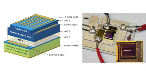
Left: Schematic outline of the prototype GaAs – InGaAs stacked solar cell with adhesive bonding layer
Right: Optical image of the fabricated and packaged GaAs – InGaAs stacked cell, the inset image shows the wire bonding to the cell bus bars
While mechanically stacked solar cells are not a new concept, the breakthrough presented by this work is the fabrication of cells using materials and process that lend themselves to wafer level processing.
BCB and Polyimide were both theoretically and experimentally investigated for solar cell bonding layers as both have been used for wafer level bonding in MEMS.
Single-junction GaAs and In0.53 Ga0.47 As solar cells with 1-Sun efficiencies of 20.6 percent and 9.3 percent were fabricated on GaAs and InP substrates respectively.
The GaAs cell was adapted for use in a stack by fabricating both p and n contacts on the front surface, to allow an insulating material to be used to bond the cells, as well as thinning the substrate to 140 µm to reduce free carrier absorption.
The InGaAs cells were fabricated with 3 µm absorber layers and featured a 100 nm thick InP window layer which helped to reduce lateral series resistance in the emitter/window region. Single cells were defined using chlorine based dry etching techniques with a SiN thin-film provided as a dual function passivation layer and anti-reflection coating.
Single-junction InGaAs cells had an open-circuit voltage of 357mV when measured under 1-sun conditions and a short-circuit current density of 38.2 mA/cm2. Benzocylobutene from the Cyclotene Advanced Electronics Resins range from Dow Corning was used as the interlayer adhesive.
The GaAs top cell was bonded to InGaAs bottom cell using a Finetech Flip-Chip bonder. It should be noted that both cells did not have matching metallisation patterns, and some negative impact on bottom cell performance was expected because of excess shading by the top cell metallisation pattern.
The bonded cells were pre-cured at 150°C under a pressure of 4 N/cm2 before the chips were cured in an oven at 210°C for 2 hours.
The Voc and Jsc values of the InGaAs cell dropped to 339 V and 19.3 mA/cm2respectively in stacked configuration. The cell contributed 4.6 percent to the efficiency of the stack leading to a total 1-sun of 25.2 percent for the dual-junction cell.
The work will be further progressed by developing a wafer scale process to investigate the commercial potential of this technique. Furthermore the concept can be extended to any solar cell type.
The next logical step for this work is the integration of III-V and Si solar cells where the silicon device will act as a low cost substrate/carrier for wide-bandgap thin-film III-V cells.
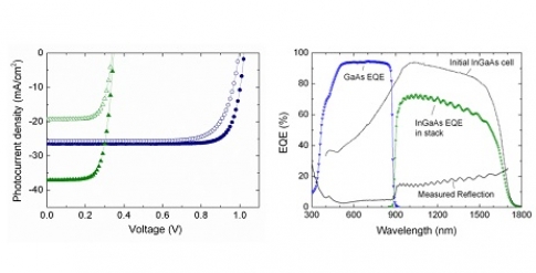
Left: Measured photocurrent density-voltage characteristics of a control GaAs cell (closed navy circles), top-contacted GaAs cell (open navy circles), stand alone InGaAs cell (green triangles) and stacked InGaAs cell (open green triangles) under 1-Sun conditions.
Right: Measured EQE of the GaAs (blue) and InGaAs (green) cells in stacked formation. Also shown is the measured reflection from the stack and the EQE of the InGaAs cell pre-bonding (black).
The details of the work described here can be found in an upcoming paper, “Adhesive bonding for mechanically stacked solar cells” by I. Mathews et al, accepted for Progress in Photovoltaics: Research and Applications, (2014).
《Adhesive bonding for mechanically stacked solar cells》:
GaAs and InGaAs solar cells in a stack have a combined efficiency of 25.2 percent
Researchers at the Tyndall National Institute, Ireland, have developed mechanically stacked solar cells (MSSC) using adhesive bonding of III-V cells.


They aim to improve the annual energy yield of concentrator photovoltaic (CPV) systems.
BCB (Benzocyclobutene) was used to bond single-junction GaAs and InGaAs solar cells in a stack with a combined efficiency of 25.2 percent under 1-Sun conditions.
The lab efficiencies of current multi-junction solar cells are achieved by designing and testing cells according to tightly defined standard solar spectra to ensure current matching between the series-connected sub-cells.
These efficiencies are rare in commercial concentrator photovoltaic (CPV) systems as the incident solar spectrum varies with the time of day, geographical location and weather conditions where the sub-cells are no longer current matched and the photocurrent produced is reduced to the lowest of any cell in the device.
Mechanically stacked solar cells provide individual connections to sub-cells in a multi-junction device. The parallel-connections remove the current matching constraint of multi-junction solar cells and potentially facilitate increased efficiency and energy yield from CPV systems as maximum power is extracted from each sub-cell at all times, independent of the incident spectrum.
Left: Schematic outline of the prototype GaAs – InGaAs stacked solar cell with adhesive bonding layer
Right: Optical image of the fabricated and packaged GaAs – InGaAs stacked cell, the inset image shows the wire bonding to the cell bus bars
While mechanically stacked solar cells are not a new concept, the breakthrough presented by this work is the fabrication of cells using materials and process that lend themselves to wafer level processing.
BCB and Polyimide were both theoretically and experimentally investigated for solar cell bonding layers as both have been used for wafer level bonding in MEMS.
Single-junction GaAs and In0.53 Ga0.47 As solar cells with 1-Sun efficiencies of 20.6 percent and 9.3 percent were fabricated on GaAs and InP substrates respectively.
The GaAs cell was adapted for use in a stack by fabricating both p and n contacts on the front surface, to allow an insulating material to be used to bond the cells, as well as thinning the substrate to 140 µm to reduce free carrier absorption.
The InGaAs cells were fabricated with 3 µm absorber layers and featured a 100 nm thick InP window layer which helped to reduce lateral series resistance in the emitter/window region. Single cells were defined using chlorine based dry etching techniques with a SiN thin-film provided as a dual function passivation layer and anti-reflection coating.
Single-junction InGaAs cells had an open-circuit voltage of 357mV when measured under 1-sun conditions and a short-circuit current density of 38.2 mA/cm2. Benzocylobutene from the Cyclotene Advanced Electronics Resins range from Dow Corning was used as the interlayer adhesive.
The GaAs top cell was bonded to InGaAs bottom cell using a Finetech Flip-Chip bonder. It should be noted that both cells did not have matching metallisation patterns, and some negative impact on bottom cell performance was expected because of excess shading by the top cell metallisation pattern.
The bonded cells were pre-cured at 150°C under a pressure of 4 N/cm2 before the chips were cured in an oven at 210°C for 2 hours.
The Voc and Jsc values of the InGaAs cell dropped to 339 V and 19.3 mA/cm2respectively in stacked configuration. The cell contributed 4.6 percent to the efficiency of the stack leading to a total 1-sun of 25.2 percent for the dual-junction cell.
The work will be further progressed by developing a wafer scale process to investigate the commercial potential of this technique. Furthermore the concept can be extended to any solar cell type.
The next logical step for this work is the integration of III-V and Si solar cells where the silicon device will act as a low cost substrate/carrier for wide-bandgap thin-film III-V cells.
Left: Measured photocurrent density-voltage characteristics of a control GaAs cell (closed navy circles), top-contacted GaAs cell (open navy circles), stand alone InGaAs cell (green triangles) and stacked InGaAs cell (open green triangles) under 1-Sun conditions.
Right: Measured EQE of the GaAs (blue) and InGaAs (green) cells in stacked formation. Also shown is the measured reflection from the stack and the EQE of the InGaAs cell pre-bonding (black).
The details of the work described here can be found in an upcoming paper, “Adhesive bonding for mechanically stacked solar cells” by I. Mathews et al, accepted for Progress in Photovoltaics: Research and Applications, (2014).